| CPC H10K 59/1213 (2023.02) [H10K 50/844 (2023.02); H10K 59/1216 (2023.02); H10K 59/131 (2023.02); H10K 71/00 (2023.02); H10K 59/1201 (2023.02)] | 20 Claims |

|
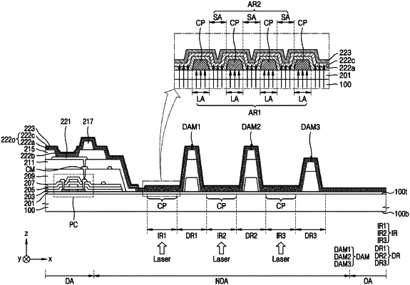
1. A method of manufacturing a display apparatus, the method comprising:
preparing a substrate in which an opening area and a non-display area around at least a portion of the opening area are defined;
forming, on the substrate, an insulating layer having an opening corresponding to the opening area and defining an irradiated region including a first area and a second area on the non-display area;
forming a conductive pattern on the irradiated region of the insulating layer, covering the first area of the insulating layer, and exposing the second area of the insulating layer;
forming an organic material layer on the insulating layer and the conductive pattern;
forming an electrode layer on the organic material layer; and
removing, by irradiating a laser beam to the irradiated region of the insulating layer, the conductive pattern, the organic material layer on the irradiated region, and the electrode layer on the irradiated region.
|