| CPC H10K 59/1213 (2023.02) [G09G 3/2003 (2013.01); G09G 3/3233 (2013.01); H10K 59/1216 (2023.02); H10K 59/126 (2023.02); H10K 59/131 (2023.02); H10K 71/00 (2023.02); G06F 3/038 (2013.01); G09G 3/30 (2013.01); G09G 2300/0426 (2013.01); G09G 2300/0443 (2013.01); G09G 2310/061 (2013.01); H01L 27/1222 (2013.01); H10K 59/1201 (2023.02); H10K 59/352 (2023.02)] | 24 Claims |
|
1. A display substrate, comprising:
a base substrate and a plurality of repeating units in an array along a first direction and a second direction on the base substrate, the first direction being intersected with the second direction,
wherein each of the plurality of repeating units comprises a first color sub-pixel, a second color sub-pixel, and a third color sub-pixel, each sub-pixel comprises an organic light emitting element and a pixel circuit for driving the organic light emitting element, and
the pixel circuit comprises a driving circuit, the driving circuit of the first color sub-pixel comprises a first driving transistor, the driving circuit of the second color sub-pixel comprises a second driving transistor, and the driving circuit of the third color sub-pixel comprises a third driving transistor, and a channel width-length ratio of the first driving transistor is greater than a channel width-length ratio of the second driving transistor and a channel width-length ratio of the third driving transistor;
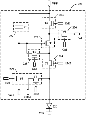
the organic light emitting element comprises a first electrode, a second electrode, and a light emitting layer between the first electrode and the second electrode, the driving circuit comprises a driving transistor, and the pixel circuit in sub-pixel of each color further comprises: a data writing transistor, a storage capacitor, a threshold compensation transistor, a first reset transistor, a second reset transistor, a first light emitting control transistor, and a second light emitting control transistor,
a first electrode of the data writing transistor is electrically connected to a first electrode of the driving transistor, a second electrode of the data writing transistor is configured to be electrically connected to a data line to receive a data signal, and a gate electrode of the data writing transistor is configured to be electrically connected to a first scanning signal line to receive a scan signal;
a first electrode of the storage capacitor is electrically connected to a first power supply terminal, and a second electrode of the storage capacitor is electrically connected to a gate electrode of the driving transistor;
a first electrode of the threshold compensation transistor is electrically connected to a second electrode of the driving transistor, a second electrode of the threshold compensation transistor is electrically connected to the gate electrode of the driving transistor, and a gate electrode of the threshold compensation transistor is configured to be electrically connected to a second scanning signal line to receive a compensation control signal;
a first electrode of the first reset transistor is configured to be electrically connected to a first reset power signal line to receive a first reset signal, a second electrode of the first reset transistor is electrically connected to the gate electrode of the driving transistor, and a gate electrode of the first reset transistor is configured to be electrically connected to a first reset control signal line to receive a first sub-reset control signal;
a first electrode of the second reset transistor is configured to be electrically connected to a second reset power signal line to receive a second reset signal, a second electrode of the second reset transistor is electrically connected to a second electrode of the organic light emitting element, and a gate electrode of the second reset transistor is configured to be electrically connected to a second reset control signal line to receive a second sub-reset control signal;
a first electrode of the first light emitting control transistor is electrically connected to the first power supply terminal, a second electrode of the first light emitting control transistor is electrically connected to the first electrode of the driving transistor, and a gate electrode of the first light emitting control transistor is configured to be electrically connected to a first light emitting control signal line to receive a first light emitting control signal; and
a first electrode of the second light emitting control transistor is electrically connected to the second electrode of the driving transistor, a second electrode of the second light emitting control transistor is electrically connected to the second electrode of the organic light emitting element, and a gate electrode of the second light emitting control transistor is configured to be electrically connected to a second light emitting control signal line to receive a second light emitting control signal.
|