US 12,069,885 B2
Display device and a method of manufacturing the same
Jeongmoon Lee, Seoul (KR); Daehong Kim, Seongnam-si (KR); and Hyungjin Lee, Suwon-si (KR)
Assigned to SAMSUNG DISPLAY CO., LTD., Yongin-si (KR)
Filed by Samsung Display Co., Ltd., Yongin-Si (KR)
Filed on Oct. 27, 2021, as Appl. No. 17/511,702.
Claims priority of application No. 10-2020-0172620 (KR), filed on Dec. 10, 2020.
Prior Publication US 2022/0190293 A1, Jun. 16, 2022
Int. Cl. H01L 51/52 (2006.01); H01L 51/56 (2006.01); H10K 50/844 (2023.01); H10K 71/00 (2023.01); H10K 71/70 (2023.01); H10K 59/122 (2023.01); H10K 59/124 (2023.01)
CPC H10K 50/844 (2023.02) [H10K 71/00 (2023.02); H10K 71/70 (2023.02); H10K 59/122 (2023.02); H10K 59/124 (2023.02)] 11 Claims
OG exemplary drawing
 
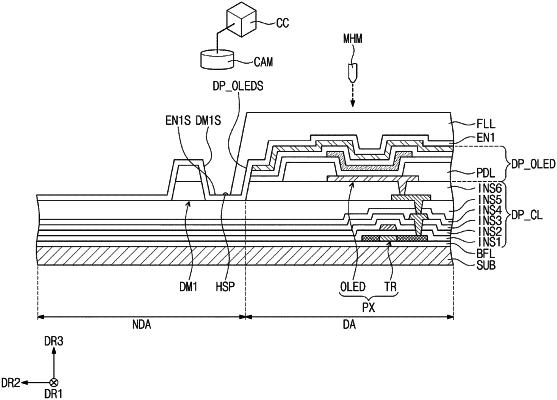
1. A display device, comprising:
a substrate;
a display element layer disposed on the substrate;
a dam disposed around the display element layer;
a plurality of patterns disposed between the dam and the display element layer; and
a planarization layer disposed on the display element layer and the patterns, wherein the patterns have a hydrophile-lipophile balance value different from a hydrophile-lipophile balance value of the planarization layer.