| CPC H10K 50/8426 (2023.02) [B32B 3/266 (2013.01); B32B 7/12 (2013.01); H10K 50/8428 (2023.02); H10K 50/86 (2023.02); H10K 71/00 (2023.02); B32B 2457/20 (2013.01)] | 6 Claims |

|
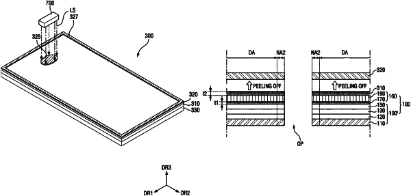
1. A display module for a display device comprising:
a display panel;
a first inter-module bonding layer disposed on an upper surface of the display panel;
a first protective film having first surface and second opposed surfaces, the first protective film being disposed on an upper surface of the first inter-module bonding layer and having a light absorbing pattern disposed on the first surface or the second surface of the first protective film; and
a through hole extending through the display panel, the first inter-module bonding layer and the first protective film,
wherein the light absorbing pattern at least partially surrounds the through hole, wherein the display panel comprises:
a display member including a substrate and a light emitting layer disposed on the substrate;
an optical film disposed on the display member; and
a second inter-module bonding layer to attach the display member and the optical film together,
wherein the first inter-module bonding layer has a first thickness and the second inter-module bonding layer has a second thickness smaller than the first thickness.
|