US 12,069,874 B2
Methods of manufacturing a field effect transistor using carbon nanotubes and field effect transistors
Marcus Johannes Henricus Van Dal, Hsinchu (TW); Timothy Vasen, Hsinchu (TW); and Gerben Doornbos, Hsinchu (TW)
Assigned to Taiwan Semiconductor Manufacturing Co., Ltd., Hsinchu (TW)
Filed by Taiwan Semiconductor Manufacturing Co., Ltd., Hsinchu (TW)
Filed on May 3, 2023, as Appl. No. 18/311,730.
Application 18/311,730 is a continuation of application No. 17/374,804, filed on Jul. 13, 2021, granted, now 11,659,721.
Application 17/374,804 is a continuation of application No. 16/590,115, filed on Oct. 1, 2019, granted, now 11,088,337, issued on Aug. 10, 2021.
Claims priority of provisional application 62/770,009, filed on Nov. 20, 2018.
Prior Publication US 2023/0276640 A1, Aug. 31, 2023
This patent is subject to a terminal disclaimer.
Int. Cl. H10K 71/60 (2023.01); H10K 10/46 (2023.01); H10K 10/84 (2023.01); H10K 19/10 (2023.01); H10K 85/20 (2023.01)
CPC H10K 10/481 (2023.02) [H10K 10/486 (2023.02); H10K 10/84 (2023.02); H10K 19/10 (2023.02); H10K 71/60 (2023.02); H10K 85/221 (2023.02)] 20 Claims
OG exemplary drawing
 
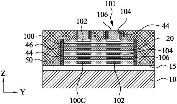
1. A method of forming a gate-all-around field effect transistor (“GAA FET”), the method comprising:
forming a fin structure over a substrate, the fin structure including a plurality of carbon nanotubes (“CNT”) each surrounded by a support layer;
releasing first portions of CNTs in the fin structure;
forming a gate structure around the first portions of the CNTs;
releasing second regions of the CNTs, the second portions extending outward from the first portions of the CNTs;
forming an inner spacer structure at least partially surrounding the second portions; and
forming a source or drain structure in contact with the second portions, the inner spacer structure between the source or drain structure and the gate structure.