| CPC H10B 99/00 (2023.02) [G11C 11/416 (2013.01)] | 16 Claims |

|
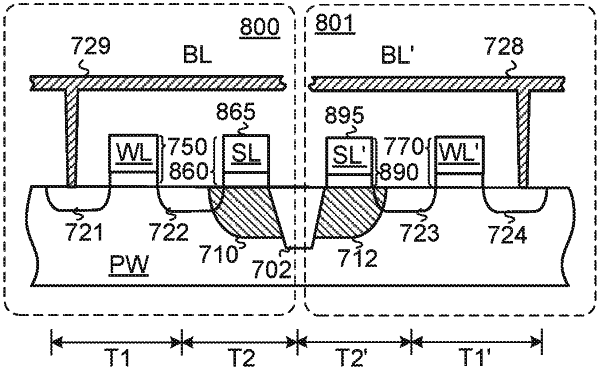
1. A cell array structure comprising a first resistive memory cell, the first resistive memory cell comprising:
a first-type well region;
a second-type first doped region formed under a surface of the first-type well region;
a second-type merged region formed under the surface of the first-type well region, wherein the second-type merged region and the first-type well region are collaboratively formed as a first diode;
a first gate structure formed over the surface of the first-type well region between the second-type first doped region and the second-type merged region, wherein the first gate structure comprises a stack structure with a first insulation layer and a first conductive layer, and the first conductive layer is served as a first word line, and wherein the second-type first doped region, the second-type merged region and the first gate structure are collaboratively formed as a first transistor;
a second gate structure formed over the second-type merged region, wherein the second gate structure comprises a stack structure with a second insulation layer and a second conductive layer, and the second conductive layer is served as a first source line, and wherein the second-type merged region and the second gate structure are collaboratively formed as a second transistor; and
a first metal layer connected with the second-type first doped region, wherein the first metal layer is served as a first bit line,
wherein a first drain/source terminal of the first transistor is connected with the first bit line, a gate terminal of the first transistor is connected with the first word line, a first drain/source terminal of the second transistor is connected with a second drain/source terminal of the first transistor, a gate terminal of the second transistor is connected to with the first source line, a body terminal of the second transistor and the first drain/source terminal of the second transistor and a second drain/source terminal of the second transistor are connected with a first terminal of the first diode, and a body terminal of the first transistor is connected with a second terminal of the first diode,
wherein during a forming action, the first source line receives a forming voltage, the first word line receives an on voltage, the first bit line receives a ground voltage, and a conducting filament is formed in the second insulation layer,
wherein during a reset action, the first source line receives a reset voltage, the first word line receives the on voltage, and the first bit line receives a first voltage lower than the reset voltage, the first transistor is turned on, the first voltage is transmitted from the first bit line to the body terminal of the second transistor and to the first drain/source terminal of the second transistor and to the second drain/source terminal of the second transistor, so that the first resistive memory cell is switched from a set state to a reset state,
wherein during a set action, the first word line receives the on voltage, the first bit line receives a set voltage, and the first source line receives a second voltage lower than the set voltage, the first transistor is turned on, the set voltage is transmitted from the first bit line to the body terminal of the second transistor and to the first drain/source terminal of the second transistor and to the second drain/source terminal of the second transistor, so that the first resistive memory cell is switched from the reset state to the set state,
wherein the reset state is corresponding to a high resistance value, the set state is corresponding to a low resistance value, and the first resistive memory cell can be arbitrarily switched between the set state and the reset state.
|