| CPC H10B 51/30 (2023.02) [G11C 8/14 (2013.01); H10B 51/10 (2023.02); H10B 51/20 (2023.02)] | 20 Claims |
|
1. A device, comprising:
a semiconductor substrate;
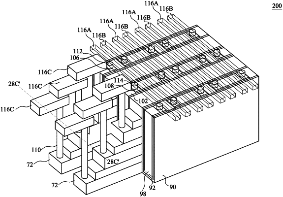
a first word line over the semiconductor substrate, the first word line providing a first gate electrode for a first transistor;
a second word line over the first word line, the second word line being insulated from the first word line by a first dielectric material, the second word line providing a second gate electrode for a second transistor over the first transistor;
a source line intersecting the first word line and the second word line;
a bit line intersecting the first word line and the second word line, the bit line being insulated from the source line by a second dielectric material;
a memory film between the first word line and the source line, the memory film further being disposed between the first word line and the bit line, wherein the memory film further extends directly under the bit line; and
a first semiconductor material between the memory film and the source line, the first semiconductor material further being disposed between the first word line and the source line, wherein the first semiconductor material further extends directly under the bit line.
|