US 12,069,863 B2
Method of forming memory device comprising conductive pillars
Yu-Wei Jiang, Hsinchu (TW); Sheng-Chih Lai, Hsinchu County (TW); TsuChing Yang, Taipei (TW); Hung-Chang Sun, Kaohsiung (TW); and Kuo-Chang Chiang, Hsinchu (TW)
Assigned to Taiwan Semiconductor Manufacturing Company, Ltd., Hsinchu (TW)
Filed by Taiwan Semiconductor Manufacturing Company, Ltd., Hsinchu (TW)
Filed on Aug. 9, 2022, as Appl. No. 17/884,536.
Application 17/884,536 is a division of application No. 17/159,179, filed on Jan. 27, 2021, granted, now 11,729,988.
Claims priority of provisional application 63/040,538, filed on Jun. 18, 2020.
Prior Publication US 2022/0384486 A1, Dec. 1, 2022
Int. Cl. H10B 51/20 (2023.01); H01L 29/24 (2006.01); H10B 51/10 (2023.01); H10B 51/30 (2023.01)
CPC H10B 51/20 (2023.02) [H01L 29/24 (2013.01); H10B 51/10 (2023.02); H10B 51/30 (2023.02)] 20 Claims
OG exemplary drawing
 
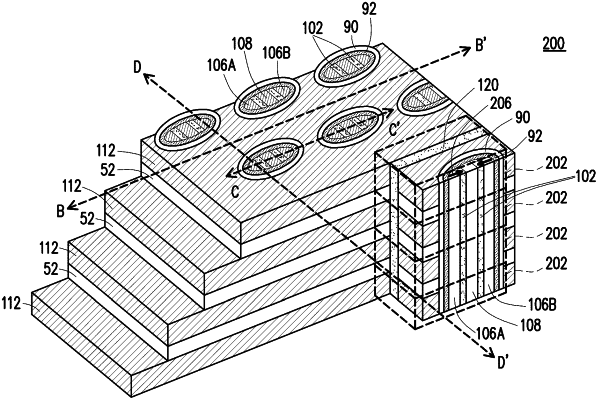
1. A method of forming a memory device, comprising:
forming a first conductive pillar;
forming a plurality of second conductive pillars at different sides of the first conductive pillar;
forming a plurality of dielectric pillars between the first conductive pillar and the plurality of second conductive pillars respectively;
forming a channel layer to continuously surround outer sidewalls of the first conductive pillar, the plurality of second conductive pillars and the plurality of dielectric pillars; and
forming a memory material layer to surround the channel layer.