| CPC H10B 43/20 (2023.02) [G11C 7/18 (2013.01); H10B 41/10 (2023.02); H10B 41/20 (2023.02); H10B 43/10 (2023.02)] | 19 Claims |

|
1. A semiconductor structure manufacturing method, comprising:
providing a substrate, and forming a plurality of bit line structures on a surface of the substrate;
forming an inter-layer dielectric layer between adjacent bit line structures, wherein an upper surface of the inter-layer dielectric layer is higher than an upper surface of the bit line structures;
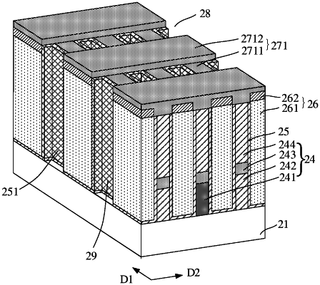
forming a first mask layer having an etching window, wherein the first mask layer comprises a first mask sublayer and a second mask sublayer, the first mask sublayer is formed on the upper surface of the bit line structures and has a plurality of strip-shaped patterns extending in a first direction and spaced apart from each other, an upper surface of the first mask sublayer is level with the upper surface of the inter-layer dielectric layer, the second mask sublayer is located on the upper surface of the first mask sublayer and the upper surface of the inter-layer dielectric layer and has a plurality of strip-shaped patterns extending in a second direction and spaced apart from each other, and the first direction is perpendicular to the second direction; and
etching the inter-layer dielectric layer by using the first mask layer as a mask, to form a contact hole, wherein the contact hole exposes the surface of the substrate.
|