| CPC H10B 12/50 (2023.02) [H10B 12/01 (2023.02)] | 20 Claims |
|
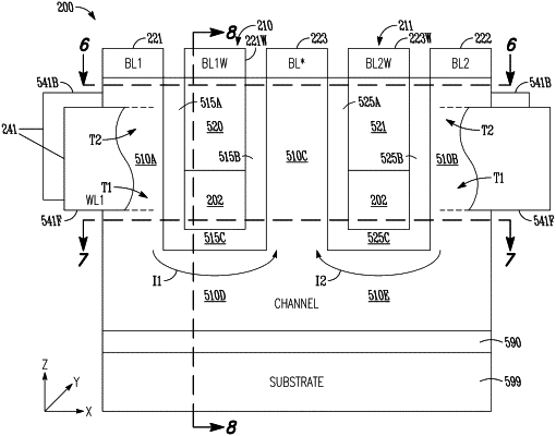
1. A method comprising:
forming a first transistor of a memory cell, including forming a charge storage structure over a substrate, and forming a first channel region from a portion of a semiconductor material, the first channel region separated from the charge storage structure by a dielectric material between the portion of the semiconductor material and the charge storage structure;
forming a second transistor of the memory cell, including forming a second channel region directly on the charge storage structure and separated from the first channel region by the dielectric material;
forming a first data line coupled to the first channel region; and
forming a second data line coupled to the first channel region, wherein the first and second data lines are formed after the first channel region is formed.
|