| CPC H10B 12/485 (2023.02) [H10B 12/34 (2023.02); H10B 12/482 (2023.02)] | 20 Claims |
|
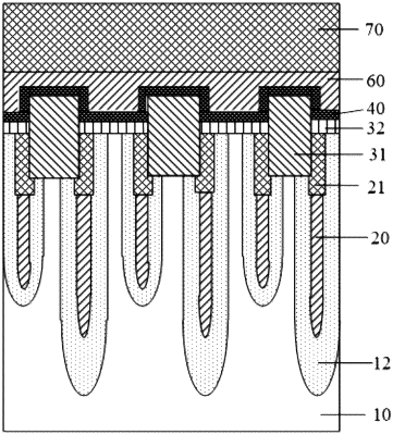
1. A semiconductor structure, comprising:
a substrate, wherein a plurality of active areas arranged in an array are provided in the substrate;
buried word lines, located in the substrate, wherein each of the active areas intersects with two of the buried word lines;
grooves, located in an upper surface of the substrate, wherein each of the grooves is located between two of the buried word lines in each of the active areas;
bit line contact layers, filling the grooves;
insulating layers, distributed between two of the grooves, wherein a thickness between upper surfaces of the insulating layers and the upper surface of the substrate is smaller than a thickness between upper surfaces of the bit line contact layers and the upper surface of the substrate; and
bit line conducting layers, covering the bit line contact layers and the insulating layers.
|