| CPC H10B 12/482 (2023.02) [H01L 21/3213 (2013.01); H01L 21/76829 (2013.01); H01L 21/76838 (2013.01); H01L 21/823468 (2013.01); H01L 29/6656 (2013.01); H10B 12/033 (2023.02); H10B 12/053 (2023.02); H10B 12/31 (2023.02); H10B 12/315 (2023.02); H10B 12/34 (2023.02)] | 19 Claims |
|
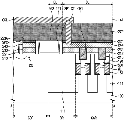
1. A semiconductor device comprising:
a substrate;
a gate structure comprising a first gate electrode, a second gate electrode and a core mask pattern which are sequentially stacked;
a plurality of cell conductive lines, each comprising a first sub-conductive line, a second sub-conductive line, a first insulating pattern, and a second insulating pattern, which are sequentially stacked;
a stack structure on the substrate between the gate structure and a first cell conductive line of the plurality of cell conductive lines, wherein the stack structure comprises a buffer pattern and a third insulating pattern on the buffer pattern;
a first spacer between the first cell conductive line and the stack structure;
a second spacer between the gate structure and the stack structure; and
a core conductive line that is on the second insulating pattern and the third insulating pattern,
wherein top surfaces of the second sub-conductive lines of the plurality of cell conductive lines are equidistant from a top surface of the substrate.
|