| CPC H10B 12/00 (2023.02) [H01L 27/1225 (2013.01); H01L 27/124 (2013.01); H01L 27/1255 (2013.01); H01L 29/24 (2013.01); H01L 29/78648 (2013.01); H01L 29/78651 (2013.01); H01L 29/7869 (2013.01)] | 12 Claims |

|
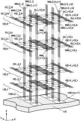
1. A memory device comprising:
N memory layers;
a driver circuit layer;
a plurality of first wirings; and
a plurality of second wirings,
wherein N is a natural number greater than or equal to 2,
wherein the N memory layers are stacked over the driver circuit layer,
wherein the driver circuit layer comprises a plurality of first circuits,
wherein the plurality of first wirings extend in a stacking direction of the N memory layers and are arranged in a matrix of P rows and R columns and P and R are each a natural number greater than or equal to 1,
wherein the plurality of second wirings extend in the stacking direction and are arranged in a matrix of P rows and Q columns and Q is a natural number greater than or equal to 2,
wherein the N memory layers each comprise:
a plurality of memory cells arranged in a matrix of P rows and Q columns;
third wirings in Q columns;
fourth wirings in Q columns; and
fifth wirings in Q columns,
wherein in the memory layer in a k-th layer:
a memory cell in an i-th row and a 2×s−1-th column and a memory cell in the i-th row and a 2×s-th column are electrically connected to a first wiring in the i-th row and an s-th column, and
the memory cell in the i-th row and the 2×s−1-th column is electrically connected to a second wiring in the i-th row and the 2×s−1-th column, a third wiring in the 2×s−1-th column, a fourth wiring in the 2×s−1-th column, and a fifth wiring in the 2×s−1-th column,
wherein the memory cell in the i-th row and the 2×s−1-th column comprises a first transistor, a second transistor, and a capacitor,
wherein one of a source and a drain of the first transistor is electrically connected to a gate of the second transistor and one electrode of the capacitor,
wherein the other of the source and the drain of the first transistor is electrically connected to the first wiring,
wherein a gate of the first transistor is electrically connected to the third wiring,
wherein the one of the source and the drain of the second transistor is electrically connected to the fourth wiring,
wherein the other of the source and the drain of the second transistor is electrically connected to the second wiring,
wherein the other electrode of the capacitor is electrically connected to the fifth wiring, and
wherein the first wiring and the second wiring are electrically connected to any one of the plurality of first circuits.
|