| CPC H05K 3/1225 (2013.01) [H05K 3/1233 (2013.01); H05K 3/24 (2013.01); H05K 1/115 (2013.01); H05K 3/282 (2013.01); H05K 3/3485 (2020.08); H05K 2203/0726 (2013.01); H05K 2203/1366 (2013.01)] | 20 Claims |
|
1. A surface mount technology (SMT) solder paste stencil, comprising:
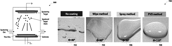
a substrate defining a plurality of solder apertures, each aperture wall of each of the plurality of solder apertures is coated with a coating material that enhances a smoothness of the each aperture wall in a SMT process and reduces wetting of a solder paste relative to the each aperture wall,
wherein the coating material has a first water contact angle greater than a second water contact angle of the substrate without the coating material,
wherein the coating material is a silicone material,
wherein the first water contact angle is greater than thirty-nine degrees and less than one hundred and ten degrees, and
wherein second water contact angle is thirty-nine degrees or less.
|