| CPC H05K 1/111 (2013.01) [G06F 1/1684 (2013.01); H05K 1/115 (2013.01); H05K 1/144 (2013.01); H05K 1/185 (2013.01); H05K 2201/096 (2013.01); H05K 2201/10378 (2013.01)] | 20 Claims |

|
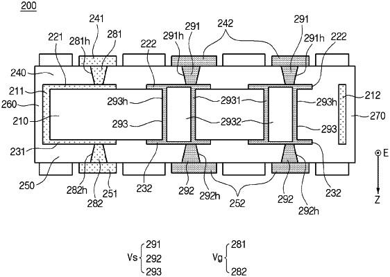
1. An electronic device comprising:
a housing;
a first board and a second board disposed in an interior of the housing and disposed to face each other in a first direction; and
an interposer extending to surround an interior space between the first board and the second board,
the interposer including:
a first conductive layer disposed to face the first board and including a first conductive area;
a second conductive layer disposed to face the second board and including a second conductive area;
an insulation layer disposed between the first conductive layer and the second conductive layer;
a first insulation part disposed between the first conductive layer and the first board and covering the first conductive area;
a second insulation part disposed between the second conductive layer and the second board and covering the second conductive area;
a first plating area extending from the first conductive layer to the second conductive layer, on a first side surface of the insulation layer;
a second plating area extending from the first conductive layer to the second conductive layer, on a second side surface of the insulation layer;
a ground via including a first part passing through the first insulation part and connected to the first conductive area, and a second part passing through the second insulation part and connected to the second conductive area, wherein the first conductive area and the second conductive area are electrically connected to each other through the first plating area; and
a signal via passing from the first insulation part to the second insulation part.
|