| CPC H05K 1/0212 (2013.01) [H01L 23/345 (2013.01); H05K 1/0224 (2013.01); H05K 1/0298 (2013.01); G11C 5/06 (2013.01); H01L 23/34 (2013.01); H05K 1/167 (2013.01); H05K 2201/10022 (2013.01); H05K 2201/10151 (2013.01); H05K 2201/10159 (2013.01)] | 7 Claims |

|
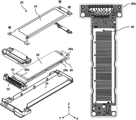
1. A storage device unit comprising:
a substrate having a main surface and having a plurality of wiring layers stacked together; and
a storage device that has a plate shape having a first major surface and a second major surface parallel and opposite to the first major surface;
wherein the plurality of wiring layers includes a heat-generating layer having a heat-generating circuit,
the first major surface of the storage device faces the main surface of the substrate,
the plurality of wiring layers includes a ground layer having a ground pattern, the ground layer is provided between the heat-generating layer and the storage device,
the plurality of wiring layers includes a layer having a thermistor, the layer having the thermistor is located between the ground layer and the storage device,
the layer having the thermistor is a layer closest to the storage device among the plurality of wiring layers, and
the thermistor is provided in a first end region of the substrate, the first end region being opposite to a second end region of the substrate in a longitudinal direction of the substrate, the second end region of the substrate being where a connector is disposed on the main surface of the substrate.
|