| CPC H04N 25/771 (2023.01) [G01S 7/4865 (2013.01); G01S 17/894 (2020.01); H04N 25/705 (2023.01); H04N 25/75 (2023.01)] | 27 Claims |

|
1. A pixel circuit, comprising:
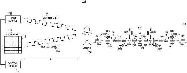
a photodiode configured to photogenerate charge in response to reflected modulated light incident upon the photodiode;
a floating diffusion configured to store a portion of the charge photogenerated in the photodiode;
a transfer transistor coupling the photodiode to the floating diffusion and configured to transfer the portion of the charge from the photodiode to the floating diffusion in response to a phase signal;
a storage node configured to store the portion of the charge from the floating diffusion;
a transistor having an input node and an output node, and coupling the floating diffusion to the storage node;
an amplifier having (i) an input coupled to the floating diffusion and to the input node of the transistor and (ii) an output coupled to a gate of the transistor; and
a reset transistor coupled between a supply rail and the input node of the transistor, wherein the reset transistor is configured to (a) reset the floating diffusion in response to a reset signal and (b) reset the storage node via the output node and the input node of the transistor.
|