| CPC H04N 25/77 (2023.01) [H01L 27/1463 (2013.01); H04N 25/75 (2023.01)] | 20 Claims |
|
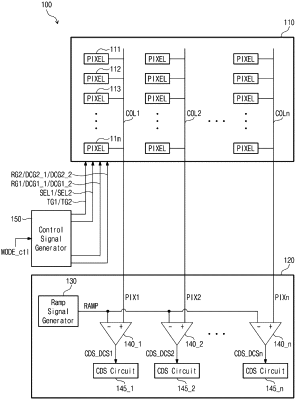
1. A pixel array comprising:
pixels arranged in a matrix shape and separated from each other by front deep trench isolation (FDTI), each of the pixels having a same structure,
wherein a first pixel among the pixels comprises:
a first floating diffusion region;
a first group of photoelectric conversion elements that are separated from each other by the FDTI;
a first group of charge transfer transistors respectively comprising vertical transfer gates, the first group of charge transfer transistors being configured to transfer photo-generated charges generated by the first group of photoelectric conversion elements to the first floating diffusion region;
a first source follower transistor comprising a first gate connected with the first floating diffusion region; and
a first transistor, a second transistor, and a first reset transistor connected in series, between the first floating diffusion region and a voltage supply line supplying a pixel power supply voltage, to adjust a first conversion gain of the first source follower transistor,
wherein a first one of the first transistor, the second transistor, and the first reset transistor is provided in a first sub-pixel region of the first pixel together with a first photoelectric conversion element among the first group of photoelectric conversion elements,
wherein a second one of the first transistor, the second transistor, and the first reset transistor, other than the first one of the first transistor, the second transistor, and the first reset transistor, is provided in a second sub-pixel region of the first pixel together with a second photoelectric conversion element among the first group of photoelectric conversion elements, and
wherein the first sub-pixel region and the second sub-pixel region are separated from each other by the FDTI.
|