| CPC H04N 25/75 (2023.01) [H04N 25/42 (2023.01); H04N 25/77 (2023.01)] | 14 Claims |
|
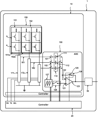
1. An analogue to digital converter for a digital imaging device comprising a plurality of pixel sensors arranged in a two-dimensional matrix comprising a plurality of columns of pixel sensors, said analogue to digital converter comprising:
a plurality of read-out capacitors, each of the plurality of read-out capacitors being associated with a respective column of pixel sensors;
a first plurality of addressable output switches, wherein each of the first plurality of addressable output switches is arranged to switchably couple an output of a pixel sensor in a column of the pixel sensor matrix to a first terminal of the read-out capacitor associated with that column;
an operational amplifier comprising an inverting input coupled to second terminals of the plurality of read-out capacitors and a non-inverting input;
a ramp signal source switchably coupled to the non-inverting input of the operational amplifier, wherein the ramp signal source is configured to output a ramping reference voltage; and
a mode selection switch arranged to switchably couple and de-couple the inverting input of the operational amplifier to a common reference voltage or the output of the operational amplifier, wherein
a controller is configured to control the first plurality of addressable switches such that the analogue to digital converter sequentially operates in a first mode of operation during which pixel sensors in a selected row of the pixel sensor matrix output reset values and a second mode of operation during which the pixel sensors in the selected row of the pixel sensor matrix output signal values, and wherein:
a. in the first mode of operation, the first plurality of addressable output switches are closed such that the pixel sensor outputs in the selected row and in each column are simultaneously connected to the first terminals of the plurality of read-out capacitors, and the mode selection switch is closed such that the inverting input of the operational amplifier is connected to the common reference voltage or to the output of the operational amplifier, such that the outputs of the pixel sensors in the row are read out in parallel and the reset values of the pixels sensors in the row are stored in their respective read-out capacitor; and
b. in the second mode of operation, the mode selection switch is opened to de-couple the inverting input from the output of the operational amplifier or the reference voltage such that the operational amplifier operates in a comparator mode, and the first plurality of addressable output switches are sequentially closed to sequentially couple the outputs of the pixel sensors in each column and in the selected row to the first terminals of their respective read-out capacitors whilst the second terminals of the plurality of read-out capacitors are coupled to the inverting input of the operational amplifier and the non-inverting input of the operational amplifier is coupled to the ramp signal source, such that for each pixel sensor whose output is sequentially coupled to the first terminal of its associated read-out capacitor, the value on the inverting input of the operational amplifier corresponds to the reset value stored in the respective read-out capacitor minus the output signal of the pixel sensor in the respective column and said value on the inverting input of the operational amplifier is rendered as a digital output value encoded by a timing with which the output of the operational amplifier toggles from one output extremum to the other.
|