| CPC H04N 25/617 (2023.01) [H01L 27/14618 (2013.01); H01L 27/14636 (2013.01); H04N 25/709 (2023.01); H04N 25/79 (2023.01)] | 22 Claims |

|
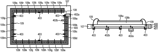
1. An imaging apparatus comprising:
an imaging device in which a plurality of photoelectric conversion elements are arranged in an array;
a wiring component in which the imaging device is mounted and a power source wiring is provided;
a plurality of connection wirings that connects the power source wiring and the imaging device each other;
at least two power supply sources connected to the power source wiring; and
at least one power supply source connected to the power source wiring,
wherein the two power supply sources and the one power supply source supply power to the imaging device via the power source wiring and the plurality of connection wirings,
wherein, at a horizontal synchronization frequency of the imaging device, the two power supply sources have lower impedances than the one power supply source, and
wherein at least one connection wiring of the plurality of connection wirings is connected to a wiring path connecting the two power supply sources in the power source wiring.
|