| CPC H04B 10/60 (2013.01) | 13 Claims |

|
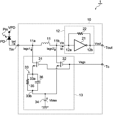
1. A receiver circuit configured to generate a voltage signal in accordance with an input current signal, the receiver circuit comprising:
an input terminal for receiving the input current signal;
a transimpedance amplifier having an input node, the transimpedance amplifier being configured to convert a current signal into the voltage signal, the current signal being input to the input node;
an inductor having a first terminal and a second terminal, the first terminal being coupled to the input terminal, the second terminal being coupled to the input node; and
a bypass circuit including:
a bias circuit configured to supply a bias voltage,
a first variable resistor coupled between the first terminal and the bias circuit,
a second variable resistor coupled between the second terminal and the bias circuit, and
an impedance adjustment circuit including a resistor and a capacitor connected in parallel to the resistor, the impedance adjustment circuit being connected in series to at least one of the first variable resistor and the second variable resistor,
wherein the impedance adjustment circuit has a cut-off frequency smaller than a half of a peak frequency, and
the receiver circuit converts the input current signal into the voltage signal with a conversion efficiency which becomes maximum at the peak frequency available when the one of the first variable resistor and the second variable resistor is set to an OFF state and the other of the first variable resistor and the second variable resistor is set to an ON state.
|