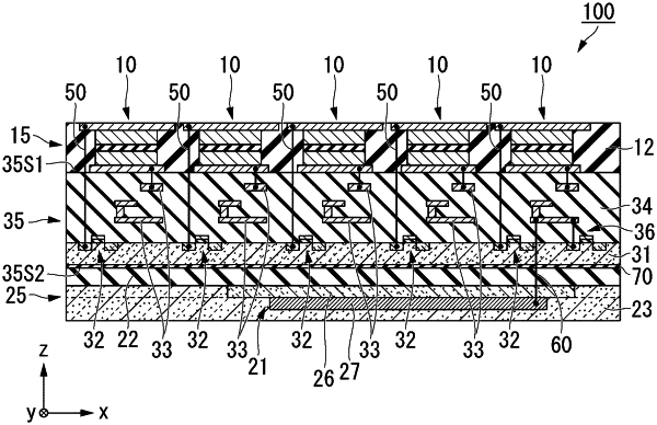
| CPC H04B 10/503 (2013.01) [H04B 10/40 (2013.01); H04B 10/532 (2013.01)] | 14 Claims |

|
1. A transceiver device comprising:
a receiving device including a magnetic element having a first ferromagnetic layer, a second ferromagnetic layer, and a spacer layer sandwiched between the first ferromagnetic layer and the second ferromagnetic layer, wherein the receiving device is configured to receive an optical signal;
a transmission device including an optical modulation element, wherein the transmission device is configured to transmit an optical signal; and
a circuit chip including an integrated circuit and an insulating layer, wherein
the optical modulation element includes a substrate having insulating properties and a waveguide provided on the substrate,
the receiving device and the transmission device are arranged on a first surface of the circuit chip and are positioned at positions where the receiving device and the transmission device do not overlap each other when viewed from a z direction which is orthogonal to the first surface of the circuit chip,
the magnetic element and the integrated circuit are electrically connected by a first through wiring which passes through the insulating layer in the z direction, and
the optical modulation element and the integrated circuit are electrically connected by a second through wiring which passes through the substrate in the z direction.
|