|
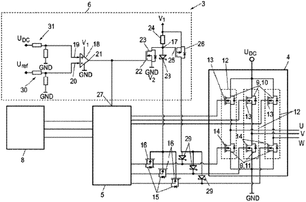
1. An electrical circuit arrangement comprising an inverter, a driver circuit and a protective circuit, wherein the inverter includes a plurality of inverter switching elements each having a drive connection, wherein the drive connection of at least one inverter switching element is connected to the driver circuit via a first switching element of the protective circuit, wherein a drive connection of the first switching element is connected to a circuit node, which is connected to a first potential via a resistor and to a second potential via a second switching element, wherein the protective circuit includes a comparison device having an input which connected to an operating voltage and a reference voltage and an output connected to a drive connection of the second switching element, so that if the operating voltage deviates from the reference voltage, the second switching element is switched and the first switching element is switched due to one of the first potential or the second potential being applied to the circuit node as a result of the switching of the second switching element.
|