| CPC H02M 1/4233 (2013.01) [H02M 1/0043 (2021.05)] | 20 Claims |

|
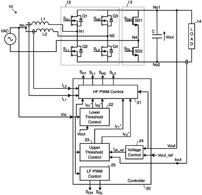
4. A power factor correction (PFC) circuit, comprising:
a first inductor coupled between a first AC voltage input mains terminal and a first node, and a second inductor coupled between the first AC voltage input mains terminal and a second node, with a second AC voltage input mains terminal coupled to a fourth node;
a first inductor current sensor coupled between the first AC voltage input mains terminal and the first inductor to thereby sense an inductor current in the first inductor, and a second inductor current sensor coupled between the first AC voltage input mains terminal and the second inductor to thereby sense an inductor current in the second inductor;
a low-frequency half-bridge coupled between first and second outputs, with a tap of the low-frequency half-bridge being the fourth node;
a high-frequency half-bridge including:
a first branch coupled between the first and second outputs, with a tap of the first branch being the first node; and
a second branch coupled between the first and second outputs, with a tap of the second branch being the second node;
an output capacitor coupled between the first and second outputs; and
a controller configured to:
generate uncompensated lower reference currents for the first and second branches, and generate uncompensated upper reference currents for the first and second branches;
generate a first control signal for the first branch based upon a comparison between the inductor current in the first inductor and the uncompensated upper and lower reference currents for the first branch;
generate a first timing reference from the first control signal for the first branch based upon a number of active slave branches, wherein the second branch is a slave branch;
generate a compensated upper reference current for the second branch by adding a first compensation current to the uncompensated upper reference current for the second branch;
generate a compensated lower reference current for the second branch by subtracting the first compensation current from the uncompensated lower reference current for the second branch;
generate a second control signal for the second branch based upon the compensated upper and lower reference current for the second branch;
generate a first timing difference based upon a phase difference between the first control signal for the first branch and the second control signal for the second branch;
generate the first compensation current based upon a difference between the first timing reference and the first timing difference; and
generate an additional control signal for switches of the low-frequency half-bridge.
|