| CPC H02H 9/005 (2013.01) [H03K 5/13 (2013.01); H03K 2005/00195 (2013.01)] | 20 Claims |

|
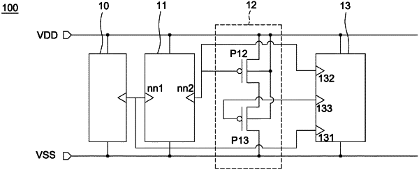
1. A power clamp device, comprising:
a delay element having an input terminal and an output terminal;
a first transistor having a gate electrically connected to the output terminal of the delay element;
a second transistor having a source electrically connected to a drain of the first transistor; and
a gate control circuit having a first terminal electrically connected to the input terminal of the delay element, a second terminal electrically connected to the output terminal of the delay element, and a third terminal electrically connected to a gate of the second transistor.
|