| CPC H01S 5/18311 (2013.01) [H01S 5/0206 (2013.01); H01S 5/0421 (2013.01); H01S 5/04254 (2019.08); H01S 5/04256 (2019.08); H01S 5/18347 (2013.01)] | 19 Claims |

|
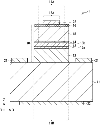
1. A surface-emitting semiconductor laser, comprising:
a substrate;
a first electrode in contact with the substrate;
a first light reflection layer over the substrate;
a second light reflection layer over the substrate, wherein the first light reflection layer is between the second light reflection layer and the substrate;
an active layer between the second light reflection layer and the first light reflection layer;
a current confining layer between the active layer and the second light reflection layer, wherein the current confining layer includes a current injection region;
a second electrode over the substrate, wherein
the second light reflection layer is between the second electrode and the substrate, and
at least a portion of the second electrode is at a position that overlaps with the current injection region; and
a contact layer between the second electrode and the second light reflection layer, wherein
the contact layer includes a contact region that is in contact with the second electrode,
a center of the contact region in a plan view is at a position that does not overlap with a center of the current injection region in the plan view,
the second light reflection layer and the contact layer have an electroconductive region at a position that overlaps with the contact region,
the electroconductive region has a higher electrical conductivity than a portion of each of the second light reflection layer and the contact layer, and
the portion of each of the second light reflection layer and the contact layer is different from the electroconductive region.
|