| CPC H01S 5/026 (2013.01) [H01S 5/04256 (2019.08); H01S 5/11 (2021.01); H01S 5/18361 (2013.01); H01S 5/343 (2013.01)] | 20 Claims |
|
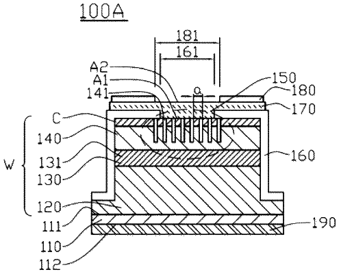
1. A laser device, comprising:
a substrate having an inner surface and an outer surface;
a first waveguiding layer over the inner surface of the substrate;
an active layer having a quantum structure over the first waveguiding layer;
a second waveguiding layer over the active layer;
a contact layer over the second waveguiding layer, wherein the first waveguiding layer, the active layer, the second waveguiding layer, and the contact layer form an epitaxy structure, the epitaxy structure having a first platform and a second platform, the first platform having multiple holes to form a photonic crystal structure;
an insulating layer over an upper surface and a sidewall surface of the first platform, and over an upper surface of the second platform, wherein the sidewall surface of the first platform passes through the contact layer, the second waveguiding layer, and the active layer, and wherein the insulating layer has an aperture corresponding to the photonic crystal structure;
a light-transmissive conducting layer over the insulating layer and connecting to the photonic crystal structure through the aperture of the insulating layer;
a first electrode over the light-transmissive conducting layer, wherein the first electrode has an opening corresponding to the aperture of the insulating layer; and
a second electrode under the outer surface of the substrate.
|