| CPC H01R 12/716 (2013.01) [H01R 12/707 (2013.01); H01R 43/0256 (2013.01); H05K 3/3405 (2013.01)] | 20 Claims |
|
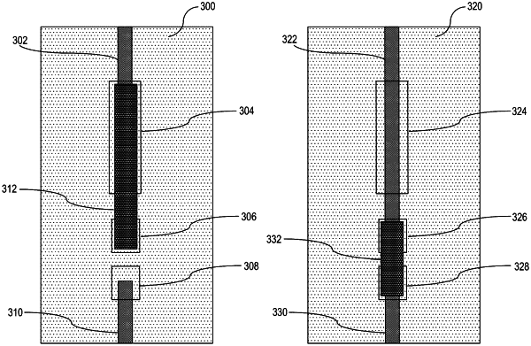
1. A dual-path signal interconnect on a printed circuit board (PCB), comprising:
a first signal trace for carrying high-speed electrical signals;
a first solder pad having a first size positioned above and connected to the first signal trace;
a second solder pad having a second size positioned above and connected to the first signal trace, wherein the second solder pad separate from the first solder pad by a first gap; and
a third solder pad having a third size, wherein the third solder pad separate from the second solder pad by a second gap and is connected to a second signal trace;
wherein the first and second solder pads are to allow a pin of an external connector to be soldered simultaneously to the first and second solder pads, such that, when the pin of the external connector is soldered, the high-speed electrical signals are routed to the external connector; and
wherein the second and third solder pads are to allow a conductor to be soldered simultaneously to the second and third solder pads, such that, when the conductor is soldered, the high-speed electrical signals are routed to the second signal trace.
|