| CPC H01R 12/585 (2013.01) [H05K 1/0271 (2013.01); H05K 1/116 (2013.01); H05K 2201/10189 (2013.01); H05K 2201/10303 (2013.01); H05K 2201/1059 (2013.01)] | 6 Claims |

|
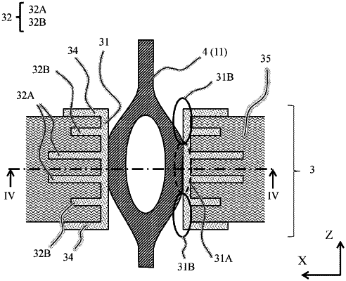
1. A circuit board assembly comprising:
a circuit board;
a through-hole into which a press-fit terminal portion is inserted in a depth direction;
an inner wall land provided on an inner wall of the through-hole; and
a plurality of inner layer lands which are provided in an inner layer of the circuit board, are planes substantially parallel to a mounting surface of the circuit board, and are in contact with the inner wall land,
wherein
the inner wall land has a first region that is in contact with the press-fit terminal portion and a second region that is not in contact with the press-fit terminal portion, and
among the plurality of inner layer lands, a first inner layer land, which is an inner layer land aligned with the first region of the inner wall land, is wider than a second inner layer land which is an inner layer land aligned with the second region of the inner wall land.
|