| CPC H01Q 9/045 (2013.01) [H01Q 5/35 (2015.01); H01Q 21/065 (2013.01)] | 20 Claims |
|
1. An electronic device comprising:
a housing configured to provide a front surface of the electronic device and a rear surface of the electronic device;
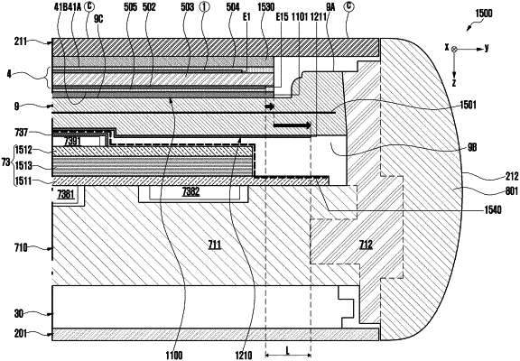
an antenna structure comprising a printed circuit board which is positioned in the housing, wherein the printed circuit board comprises:
a first surface configured to face the front surface or the rear surface,
a second surface configured to face a direction opposite to the first surface,
a first conductive layer comprising a first antenna element and a second antenna element which are configured so as not to overlap each other when viewed from above the first surface,
a second conductive layer positioned closer to the second surface than the first conductive layer and configured to operate as a ground plane, and
a dielectric positioned between the first conductive layer and the second conductive layer;
a first conductive material positioned between the front surface and the second surface when the first surface faces the rear surface and positioned between the rear surface and the second surface when the first surface faces the front surface, and configured to overlap the second conductive layer when viewed from above the first surface; and
a second conductive material positioned closer to the front surface than the first conductive material when the first surface faces the rear surface and positioned closer to the rear surface than the first conductive material when the first surface faces the front surface, and configured to overlap the first conductive material when viewed from above the first surface,
wherein when viewed from above the first surface, the second conductive layer comprises a second edge configured to correspond to a first edge of the first antenna element or the second antenna element and the second conductive material comprises a third edge configured to correspond to the second edge, and the second edge is positioned between the first edge and the third edge.
|