| CPC H01L 33/502 (2013.01) [H01L 25/0753 (2013.01); H01L 33/40 (2013.01)] | 18 Claims |
|
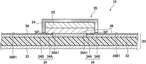
1. A phosphor substrate having at least one light emitting element mounted on one surface, the phosphor substrate comprising:
an insulating substrate;
an electrode layer disposed on one surface of the insulating substrate and bonded to the light emitting element; and
a phosphor layer which is disposed on the one surface of the insulating substrate and includes a phosphor in which a light emission peak wavelength, in a case where light emitted by the light emitting element is used as excitation light, is in a visible light region; and
an electronic component which is not the light emitting element and is mounted on the one surface of the insulating substrate,
wherein a surface of the electrode layer facing an outer side in a thickness direction of the insulating substrate is a flat surface, and
at least a part of the phosphor layer is disposed around a bonded portion of the electrode layer with the light emitting element.
|