| CPC H01L 33/387 (2013.01) [H01L 33/06 (2013.01); H01L 33/38 (2013.01)] | 31 Claims |

|
1. A light emitting element comprising:
a semiconductor structure;
first and second electrodes formed above the semiconductor structure; and
a protective film, wherein:
in a plan view:
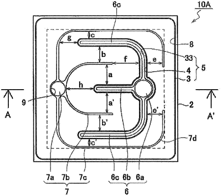
the first electrode consists of a first pad electrode configured to be bonded with a first conductive wire and electrically connected to a first external electrode or a first external terminal, a first extending portion extending from the first pad electrode, and two second extending portions extending from the first pad electrode,
the second electrode consists of a second pad electrode configured to be bonded with a second conductive wire and electrically connected to a second external electrode or a second external terminal, and two third extending portions extending from the second pad electrode,
the first extending portion extends linearly in a direction from the first pad electrode toward the second pad electrode,
the two second extending portions are located on opposite sides of the first extending portion, respectively, with each of the second extending portions having two bent portions and a linear portion extending parallel to the first extending portion and located between the two bent portions, and
the two third extending portions are located between the first extending portion and the two second extending portions, respectively, and
the protective film covers the first extending portion, the two second extending portions, and the two third extending portions, while the first pad electrode and the second pad electrode are exposed from the protective film.
|