| CPC H01L 33/382 (2013.01) [H01L 25/0753 (2013.01); H01L 27/156 (2013.01); H01L 33/005 (2013.01); H01L 2933/0016 (2013.01)] | 11 Claims |
|
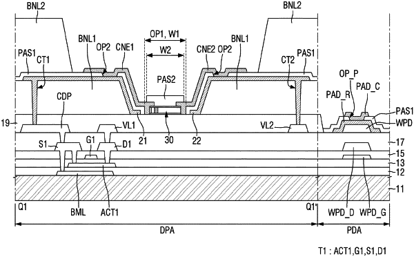
1. A display device comprising:
a planarization layer disposed on a substrate;
a first alignment electrode and a second alignment electrode that extend in a first direction and are spaced apart from each other on the planarization layer;
a first insulating layer disposed on the first alignment electrode and the second alignment electrode, the first insulating layer comprising a first opening exposing-over the planarization layer between the first alignment electrode and the second alignment electrode;
a light-emitting element disposed on the planarization layer overlapping the first opening;
a first contact electrode and a second contact electrode disposed on the first insulating layer, the first contact electrode electrically contacting a first end of the light-emitting element and the second contact electrode electrically contacting a second end of the light-emitting element; and
a second insulating layer disposed on the light-emitting element, wherein
the first contact electrode, the second contact electrode, and the light-emitting element contact the planarization layer.
|