US 12,068,434 B2
Semiconductor device and semiconductor unit
Tatehito Kobayashi, Kanagawa (JP)
Assigned to Sony Semiconductor Solutions Corporation, Kanagawa (JP)
Appl. No. 17/430,392
Filed by SONY SEMICONDUCTOR SOLUTIONS CORPORATION, Kanagawa (JP)
PCT Filed Feb. 7, 2020, PCT No. PCT/JP2020/004789
§ 371(c)(1), (2) Date Aug. 12, 2021,
PCT Pub. No. WO2020/170855, PCT Pub. Date Aug. 27, 2020.
Claims priority of application No. 2019-027481 (JP), filed on Feb. 19, 2019.
Prior Publication US 2022/0149235 A1, May 12, 2022
Int. Cl. H01L 21/00 (2006.01); H01L 25/13 (2006.01); H01L 33/20 (2010.01); H01L 33/62 (2010.01)
CPC H01L 33/20 (2013.01) [H01L 25/13 (2013.01); H01L 33/62 (2013.01)] 14 Claims
OG exemplary drawing
 
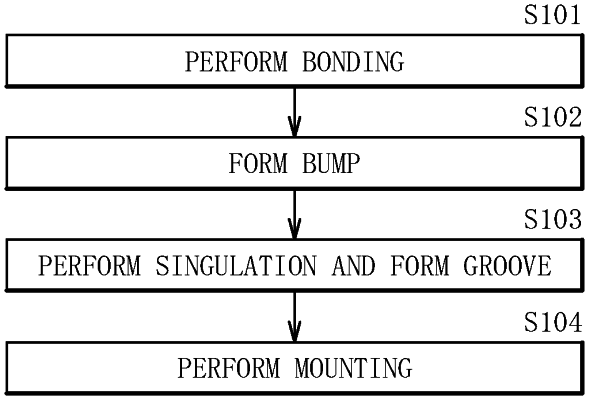
1. A semiconductor device, comprising:
a semiconductor substrate having one surface and another surface opposed to each other;
a single or multiple bumps provided on the other surface; and
a projection-and-depression structure formed in a side surface of the semiconductor substrate, wherein the side surface of the semiconductor substrate has a hydrophilic property.