| CPC H01L 33/0037 (2013.01) [H01L 27/153 (2013.01); H01L 33/62 (2013.01)] | 4 Claims |
|
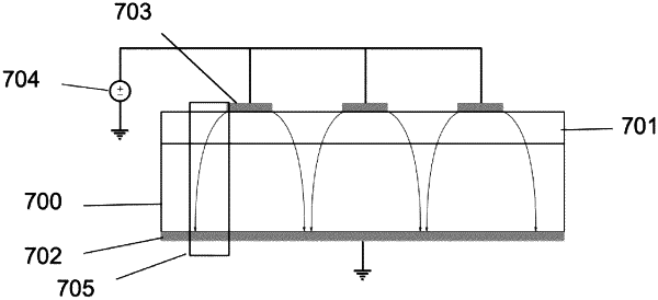
1. A method of creating an array of current driven devices in a continuous semiconductor bulk by resistance engineering, the resistance engineering including:
forming device layers on a substrate;
forming an array of contact pads on top of the device layers;
forming a metal-insulator-semiconductor structure around the contact pads;
after the forming the device layers, the array of contact pads, and the metal-insulator-semiconductor structure, manipulating a resistance of an area of a conductive top layer between adjacent contact pads within the continuous semiconductor bulk to limit lateral current flow components; and
after the forming the device layers, the array of contact pads, and the metal-insulator-semiconductor structure, biasing the metal-insulator-semiconductor structure to force current vertically in the device layers.
|