| CPC H01L 29/788 (2013.01) [H01L 29/42328 (2013.01); H01L 29/42336 (2013.01); H01L 29/6656 (2013.01); H01L 29/66825 (2013.01); H10B 41/35 (2023.02); H10B 41/41 (2023.02)] | 15 Claims |

|
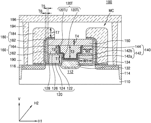
1. An integrated circuit (IC) device comprising:
a source region arranged in an upper portion of a substrate;
a pair of split gate structures respectively on opposing sides of the source region, wherein each of the pair of split gate structures includes a floating gate electrode layer and control gate electrode layers disposed on the floating gate electrode layer;
an erase gate structure between the pair of split gate structures on the source region and including an erase gate electrode layer;
a gate capping layer extending across an upper surface of the erase gate structure;
a pair of selection gate structures respectively on outer sidewalls of the pair of split gate structures; and
a pair of gate spacers, wherein each gate spacer of the pair of gate spacers is disposed between one of the pair of split gate structures and one of the pair of selection gate structures, includes a first gate spacer and a second gate spacer disposed on the first gate spacer, is further disposed on an outer side wall of the one of the pair of split gate structures, and a lowermost end of the second gate spacer is at a lower level than an upper surface of the floating gate electrode layer,
wherein each selection gate structure of the pair of selection gate structures comprises a selection gate insulating layer contacting the second gate spacer and a top surface of the gate capping layer.
|