| CPC H01L 29/7842 (2013.01) [H01L 21/02304 (2013.01); H01L 21/02507 (2013.01); H01L 29/0665 (2013.01); H01L 29/41791 (2013.01); H01L 29/66795 (2013.01); H01L 29/785 (2013.01)] | 20 Claims |

|
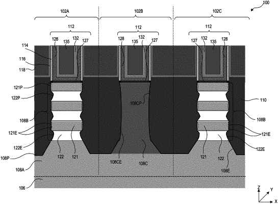
1. A method, comprising:
forming a fin structure on a substrate;
forming a superlattice structure on the fin structure, comprising first and second nanostructured layers;
forming an opening in the superlattice structure and in the fin structure, wherein first, second, and third surfaces of the first nanostructured layers, second nanostructured layers, and fin structure, respectively, are exposed within the opening;
modifying the first surfaces of the first nanostructured layers to curve a profile of the first surfaces;
depositing first, second, and third passivation layers on the first, second, and third surfaces, respectively, wherein the first, second, and third passivation layers are different from each other; and
forming an epitaxial source/drain (S/D) region on the superlattice structure.
|