| CPC H01L 29/7786 (2013.01) [G01R 19/0092 (2013.01); G01R 31/2621 (2013.01); H01L 29/2003 (2013.01)] | 19 Claims |

|
1. A SenseHEMT comprising:
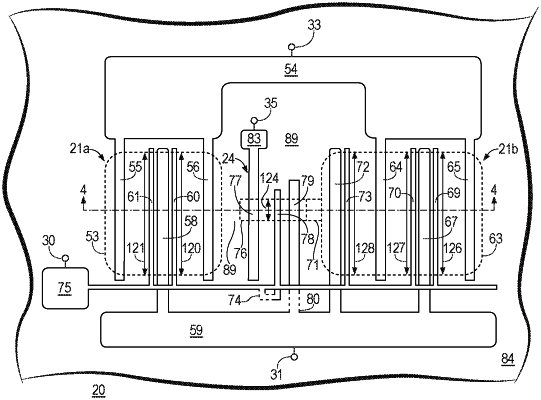
a GaN transistor having a main transistor and a sense transistor formed on a semiconductor substrate, the main transistor having a main active area and the sense transistor having a sense active area;
an isolation structure that isolates the sense active area from the main active area;
a main drain of the main transistor within the main active area;
a sense gate of the sense transistor in the sense active area, the sense gate having a first width;
a sense drain of the sense transistor in the sense active area;
a main gate of the main transistor in the main active area, the main gate having a second width that is greater than the first width, the main gate connected to the sense gate;
a sense source of the sense transistor in the sense active area; and
a main source of the main transistor in the main active area wherein one of the main source is connected to the sense source or the main drain is connected to the sense drain.
|