| CPC H01L 29/7786 (2013.01) [H01L 29/0607 (2013.01); H01L 29/2003 (2013.01); H01L 29/66462 (2013.01)] | 20 Claims |
|
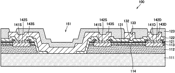
1. A semiconductor device, comprising:
a semiconductor substrate;
a channel layer that is formed on the semiconductor substrate and that includes a first compound semiconductor;
a barrier layer that is formed on the channel layer and that includes a second compound semiconductor that is different from the first compound semiconductor;
a gate electrode provided on the barrier layer via a gate insulating film;
a source electrode and a drain electrode provided on the channel layer with the gate electrode interposed therebetween;
a substrate opening that penetrates the channel layer and exposes the semiconductor substrate;
an insulating film provided from upper parts of the gate electrode, the source electrode, and the drain electrode to an inner side of the substrate opening; and
a wiring line layer provided on the insulating film and electrically coupled to one of the gate electrode, the source electrode, and the drain electrode via an opening provided on the insulating film,
wherein at least a portion of the substrate opening is formed in an activation region in which the gate electrode, the source electrode, and the drain electrode are provided,
wherein the substrate opening is formed in the activation region positioned on the source electrode side with respect to the gate electrode,
wherein the source electrode is divided by the substrate opening, and
wherein the divided source electrode is electrically coupled by the wiring line layer formed at the inner side of the substrate opening.
|