| CPC H01L 29/7786 (2013.01) [H01L 29/1066 (2013.01); H01L 29/402 (2013.01); H01L 29/66462 (2013.01); H01L 29/7787 (2013.01); H01L 29/2003 (2013.01)] | 20 Claims |
|
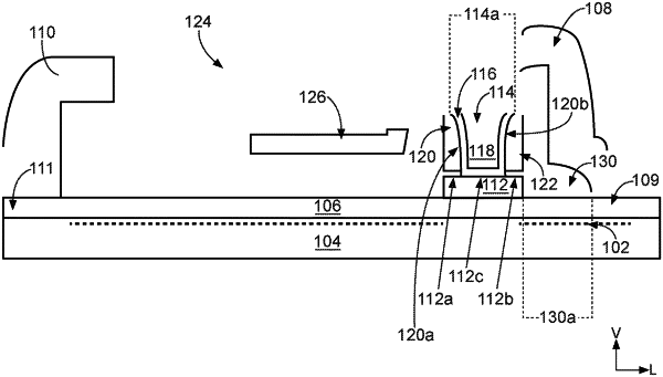
1. A High Electron Mobility Transistor (HEMT), comprising:
a source;
a drain;
a channel layer extending between the source and the drain;
a barrier layer formed in contact with the channel layer, and extending between the source and the drain;
a p-type gate formed in contact with, and covering at least a portion of, the barrier layer, the gate having gate edge portions and a gate central portion;
dielectric spacers formed over the gate edge portions, the dielectric spacers having a first total width therebetween at a first distance from the gate, and a second total width therebetween at a second distance from the gate, the second total width being longer than the first total width and the second distance being longer than the first distance; and
a gate electrode formed on the gate central portion and between the dielectric spacers.
|