| CPC H01L 29/7397 (2013.01) [H01L 29/0607 (2013.01); H01L 29/41708 (2013.01); H01L 29/861 (2013.01)] | 20 Claims |

|
1. A semiconductor device, comprising:
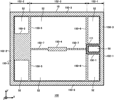
a semiconductor substrate that has, in a top view, one set of first end sides facing each other in a first direction and one set of second end sides facing each other in a second direction;
a first electrode that is provided above the semiconductor substrate and configured with metal;
one or more pads that are provided to be separated from the first electrode above the semiconductor substrate and configured with metal; and
a beam portion that is provided above the semiconductor substrate, and is configured with an insulating material, wherein
the beam portion has
a peripheral beam portion that is provided along the first end sides and the second end sides,
at least one first beam portion that extends in the second direction and adjacently past the one or more pads, one end and other end of the at least one beam portion being connected to the peripheral beam portion, and
at least one second beam portion that extends in the first direction.
|