| CPC H01L 29/737 (2013.01) [H01L 29/66242 (2013.01)] | 19 Claims |
|
1. A method of forming an integrated circuit, the method comprising:
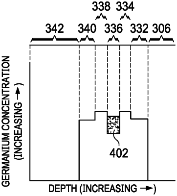
epitaxially growing a first sub-layer of a base region on or over a collector region, the first sub-layer having a first uniform concentration of a semiconductor species, the collector region being disposed on or over a semiconductor substrate;
epitaxially growing a second sub-layer of the base region on or over the first sub-layer, the second sub-layer having a second uniform concentration of the semiconductor species, said epitaxially growing the second sub-layer comprising doping the second sub-layer with a first dopant; and
epitaxially growing a third sub-layer of the base region on or over the second sub-layer, the third sub-layer having a third uniform concentration of the semiconductor species, the second concentration less than the first concentration and less than the third concentration.
|