| CPC H01L 29/6681 (2013.01) [H01L 21/31055 (2013.01); H01L 21/823418 (2013.01); H01L 21/823431 (2013.01); H01L 21/823468 (2013.01); H01L 29/6653 (2013.01); H01L 29/66545 (2013.01); H01L 29/6656 (2013.01)] | 20 Claims |

|
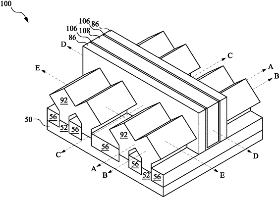
1. A method for making a semiconductor device, comprising:
forming a first gate stack over a first fin;
forming a first gate spacer extending along a side of the first gate stack, the first gate spacer comprising a first dielectric material;
forming a second gate spacer over the first gate spacer, the second gate spacer comprising silicon germanium;
forming a third gate spacer over the second gate spacer, the third gate spacer comprising a second dielectric material;
forming a source/drain region adjacent the third gate spacer;
depositing an interlayer dielectric (ILD) over the source/drain region, the ILD comprising a third dielectric material; and
removing at least a portion of the second gate spacer to form a void, while exposing a top surface of the ILD,
wherein the step of removing at least a portion of the second gate spacer leaves the first gate spacer, the third gate spacer, and the ILD intact.
|