| CPC H01L 29/6681 (2013.01) [H01L 21/823431 (2013.01); H01L 27/0924 (2013.01); H01L 29/7851 (2013.01)] | 20 Claims |
|
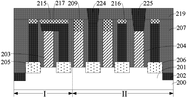
1. A semiconductor structure, comprising:
a substrate, wherein the substrate includes a first region and a second region adjacent to the first region;
a first gate structure and first source-drain doped layers, wherein the first gate structure is formed over the first region, and the first source-drain doped layers are formed in the first region of the substrate on both sides of the first gate structure, respectively;
a second gate structure and second source-drain doped layers, wherein the second gate structure is formed over the second region, and the second source-drain doped layers are formed in the second region of the substrate on both sides of the second gate structure, respectively;
a first protection layer, formed over the second gate structure;
a first conductive structure, formed over a first source-drain doped layer of the source-drain doped layers, wherein the first conductive structure is also formed on the first gate structure, a top surface of the first conductive structure is lower than a top surface of the first protection layer; and
an isolation layer, formed over the first conductive structure, a top surface of the isolation layer over the first conductive structure being coplanar with the top surface of the first protection layer over second gate structure.
|