| CPC H01L 29/66795 (2013.01) [H01L 21/32136 (2013.01); H01L 21/823431 (2013.01); H01L 29/0653 (2013.01); H01L 29/7851 (2013.01)] | 20 Claims |
|
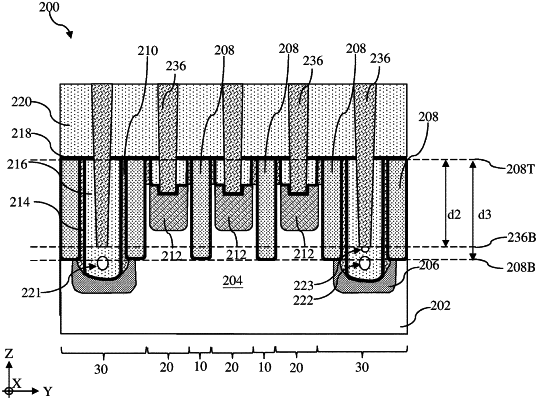
1. A semiconductor structure, comprising:
a first fin structure and a second fin structure arising from a substrate;
an isolation feature disposed between the first fin structure and the second fin structure;
a first epitaxial source/drain feature disposed over the first fin structure;
a second epitaxial source/drain feature disposed over the second fin structure;
a contact etch stop layer (CESL) disposed over the isolation feature;
an interlayer dielectric (ILD) layer over the CESL; and
a source/drain contact extending through the CESL and the ILD layer to electrically couple to first epitaxial source/drain feature and the second epitaxial source/drain feature,
wherein a portion of the source/drain contact extends between the first epitaxial source/drain feature and the second epitaxial source/drain feature,
wherein a bottom surface of the first epitaxial source/drain feature is lower than a bottom surface of the portion of the source/drain contact that extends between the first epitaxial source/drain feature and the second epitaxial source/drain feature.
|