| CPC H01L 29/66795 (2013.01) [H01L 21/3065 (2013.01); H01L 21/30655 (2013.01); H01L 21/3085 (2013.01); H01L 21/31116 (2013.01); H01L 21/76232 (2013.01); H01L 29/785 (2013.01); H01L 29/7851 (2013.01); H01L 29/7853 (2013.01)] | 20 Claims |
|
1. A semiconductor device, comprising:
a substrate;
a fin structure protruding from an isolation insulating layer disposed over the substrate;
a gate insulating layer covering a channel region formed of the fin structure; and
a gate electrode layer covering the gate insulating layer;
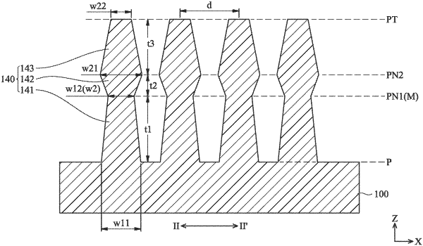
wherein the fin structure includes a bottom portion, a neck portion, and a top portion sequentially disposed on the substrate,
the neck portion has an arcuate surface,
an angle θ1 between a side surface of the bottom portion and a horizontal plane is an acute angle,
an angle θ3 between a side surface of the top portion and a horizontal plane is substantially a right angle,
a width of an uppermost portion of the fin structure is greater than a width of a narrowest portion of the neck portion,
the narrowest portion of the neck portion is below a lowermost portion of the gate electrode layer along a direction in which the fin structure protrudes from the substrate,
a width of the top portion decreases along a direction in which the fin structure protrudes from the substrate.
|