| CPC H01L 29/42316 (2013.01) [H01L 23/4821 (2013.01); H01L 23/4824 (2013.01); H01L 23/66 (2013.01); H01L 29/0692 (2013.01); H01L 29/802 (2013.01)] | 2 Claims |

|
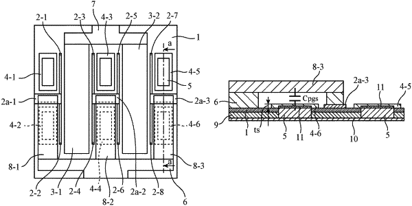
1. A semiconductor device comprising:
a semiconductor layer disposed on a substrate;
at least one gate connecting portion disposed on the semiconductor layer;
a plurality of gate fingers extending symmetrically from both sides of the at least one gate connecting portion;
a drain electrode adjacent to both one of the plurality of gate fingers which extends from a first side of the at least one gate connecting portion and another one of the plurality of gate fingers which extends from a second side of the at least one gate connecting portion, the second side being opposite to the first side;
a plurality of source electrodes respectively adjacent to a gate finger among the plurality of gate fingers extending from the first side of the at least one gate connecting portion and another gate finger among the plurality of gate fingers extending from the second side of the at least one gate connecting portion;
a gate routing line via which electric power to be inputted to the plurality of gate fingers is transmitted;
a gate air bridge connecting the at least one gate connecting portion and the gate routing line while straddling a source electrode among the plurality of source electrodes adjacent to said another gate finger extending from the second side of the at least one gate connecting portion; and a metal layer disposed under each of the plurality of source electrodes and having etching resistance higher than etching resistance of the plurality of source electrodes, wherein
the metal layer comprises a first length in a longitudinal direction of the metal layer, and each of the source electrodes comprises a second length in a longitudinal direction of the source electrode, and
the first length of the metal layer is less than the second length of each of the source electrodes.
|