| CPC H01L 29/41791 (2013.01) [H01L 21/823418 (2013.01); H01L 21/823431 (2013.01); H01L 21/823468 (2013.01); H01L 21/823481 (2013.01); H01L 21/823814 (2013.01); H01L 21/823821 (2013.01); H01L 21/845 (2013.01); H01L 27/0886 (2013.01); H01L 27/0924 (2013.01); H01L 27/1211 (2013.01); H01L 29/0649 (2013.01); H01L 29/41725 (2013.01); H01L 29/41783 (2013.01); H01L 29/456 (2013.01); H01L 29/6656 (2013.01); H01L 29/66575 (2013.01); H01L 29/66636 (2013.01); H01L 29/66772 (2013.01); H01L 29/66795 (2013.01); H01L 29/7831 (2013.01); H01L 29/785 (2013.01); H10B 12/056 (2023.02); H01L 29/66545 (2013.01)] | 20 Claims |
|
1. A semiconductor device comprising:
a substrate;
a dielectric isolation region extending into the substrate;
a semiconductor strip between and contacting opposing portions of the dielectric isolation region;
a gate structure on the substrate;
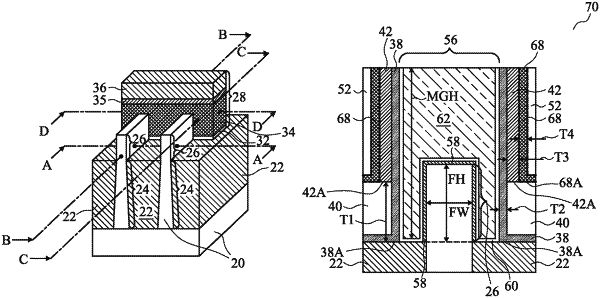
a first spacer adjacent to and directly contacting the gate structure, wherein the first spacer comprises silicon carbo-nitride (SiCN), and the first spacer has an L-shape;
a second spacer adjacent to and directly contacting the first spacer, wherein the second spacer comprises silicon oxycarbonitride (SiOCN), and wherein the second spacer comprises;
a vertical-and-straight inner edge; and
an outer edge comprising a vertical-and-straight portion;
a source/drain region adjacent to two sides of the second spacer, wherein the source/drain region overlaps the semiconductor strip, and wherein the source/drain region comprises:
a first vertical-and-straight sidewall; and
a second vertical-and-straight sidewall parallel to the first vertical-and-straight sidewall, wherein the source/drain region is wider than the semiconductor strip; and
a top dielectric layer over and contacting a top surface of the dielectric isolation region, wherein the top dielectric layer comprises SiCN, wherein the top dielectric layer further extends directly underlying the source/drain region.
|