| CPC H01L 29/2003 (2013.01) [H01L 21/8232 (2013.01); H01L 29/41758 (2013.01); H01L 29/778 (2013.01); H01L 29/808 (2013.01); H01L 29/812 (2013.01); H01L 29/861 (2013.01)] | 8 Claims |
|
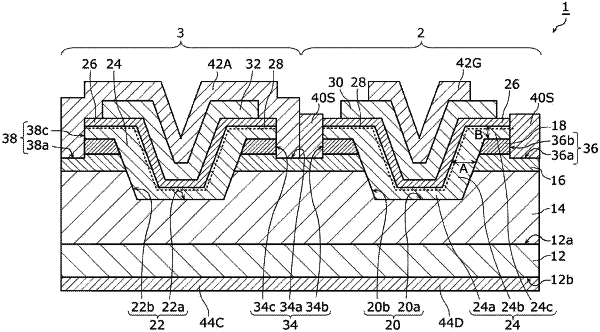
1. A nitride semiconductor device including a vertical transistor and a vertical diode, the nitride semiconductor device comprising:
a substrate;
a first nitride semiconductor layer of a first conductivity type above the substrate;
a second nitride semiconductor layer of a second conductivity type above the first nitride semiconductor layer, the second conductivity type being different from the first conductivity type;
a first opening penetrating through the second nitride semiconductor layer to the first nitride semiconductor layer;
a second opening provided away from the first opening and penetrating through the second nitride semiconductor layer to the first nitride semiconductor layer;
an electron transport layer and an electron supply layer provided, in stated order from a substrate side, along an inner face of each of the first opening and the second opening and above the second nitride semiconductor layer;
a gate electrode of the vertical transistor above the electron supply layer and covering the first opening;
an anode electrode of the vertical diode above the electron supply layer and covering the second opening;
a third opening provided between the first opening and the second opening in a plan view and penetrating through the electron supply layer and the electron transport layer to the second nitride semiconductor layer;
a source electrode of the vertical transistor connected to the second nitride semiconductor layer and a portion of each of the electron supply layer and the electron transport layer on a first opening side, in the third opening;
a drain electrode of the vertical transistor provided on a side of the substrate facing away from the first nitride semiconductor layer, at a position where the drain electrode overlaps the gate electrode in a plan view; and
a cathode electrode of the vertical diode on the side of the substrate facing away from the first nitride semiconductor layer, at a position where the cathode electrode overlaps the anode electrode in a plan view,
wherein the anode electrode and the source electrode are electrically connected, and
the cathode electrode and the drain electrode are electrically connected.
|