| CPC H01L 29/1029 (2013.01) [H01L 29/045 (2013.01); H01L 29/2003 (2013.01); H01L 29/66462 (2013.01); H01L 29/7786 (2013.01)] | 23 Claims |
|
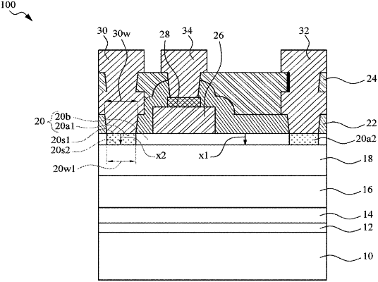
1. A semiconductor device, comprising:
a substrate;
a first nitride semiconductor layer on the substrate;
a second nitride semiconductor layer on the first nitride semiconductor layer and having a bandgap greater than a bandgap of the first nitride semiconductor layer, the second nitride semiconductor layer having a first area and a second area, and the second nitride semiconductor layer having a single crystal structure; and
an electrode in contact with the first area,
wherein a first concentration of an element in the first area is less than a second concentration of the element in the second area, the second area comprises the element gradientially distributed along a direction toward the first nitride semiconductor layer, and wherein the single crystal structure in the first area takes over a crystal structure in the first nitride semiconductor layer.
|